| CPC H01L 29/7848 (2013.01) [H01L 29/0649 (2013.01); H01L 29/0673 (2013.01); H01L 29/0676 (2013.01); H01L 29/165 (2013.01); H01L 29/42392 (2013.01); H01L 29/66439 (2013.01); H01L 29/66537 (2013.01); H01L 29/66545 (2013.01); H01L 29/66795 (2013.01); H01L 29/775 (2013.01); H01L 29/7851 (2013.01); H01L 29/78696 (2013.01)] | 20 Claims |
|
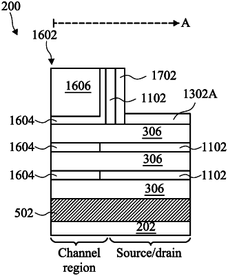
1. A multi-gate semiconductor device, comprising:
a fin element extending from a substrate;
a plurality of nanowire channel layers including a first nanowire channel layer, disposed over the fin element and a second nanowire channel layer over the first nanowire channel layer;
a first portion of a high-k gate dielectric material extending between the first nanowire channel layer and the second nanowire channel layer and a second portion of the high-k gate dielectric material extending between the first nanowire channel layer and the fin element;
a spacer layer adjacent the first portion of the high-k gate dielectric material and adjacent the second portion of the high-k gate dielectric material; and
a gate electrode disposed over the plurality of nanowire channel layers.
|