US 11,942,547 B2
Source/drain epitaxial layer profile
Gulbagh Singh, Tainan (TW); Hsin-Chi Chen, Tainan (TW); and Kun-Tsang Chuang, Miaoli (TW)
Assigned to Taiwan Semiconductor Manufacturing Co., Ltd., Hsinchu (TW)
Filed by Taiwan Semiconductor Manufacturing Co., Ltd., Hsinchu (TW)
Filed on Jul. 26, 2022, as Appl. No. 17/815,063.
Application 17/815,063 is a division of application No. 17/031,530, filed on Sep. 24, 2020, granted, now 11,462,642, issued on Oct. 4, 2022.
Application 17/031,530 is a division of application No. 16/117,064, filed on Aug. 30, 2018, granted, now 10,790,391, issued on Sep. 29, 2020.
Claims priority of provisional application 62/690,648, filed on Jun. 27, 2018.
Prior Publication US 2022/0359751 A1, Nov. 10, 2022
Int. Cl. H01L 29/78 (2006.01); H01L 21/02 (2006.01); H01L 21/265 (2006.01); H01L 21/3065 (2006.01); H01L 21/762 (2006.01)
CPC H01L 29/7846 (2013.01) [H01L 21/02532 (2013.01); H01L 21/26513 (2013.01); H01L 21/3065 (2013.01); H01L 21/76237 (2013.01)] 20 Claims
OG exemplary drawing
 
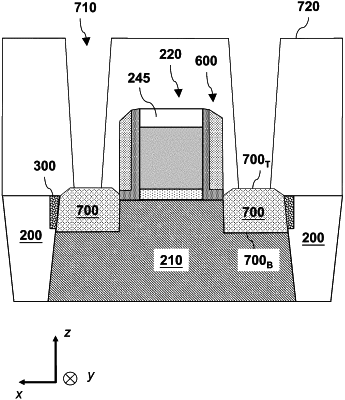
1. A semiconductor structure, comprising:
a semiconductor layer on a substrate;
an isolation region surrounding the semiconductor layer;
an epitaxial stack partially disposed in the semiconductor layer; and
a germanium-doped (Ge-doped) structure on the semiconductor layer and between the isolation region and the epitaxial stack, wherein a depth of the epitaxial stack is equal to or greater than a depth of the Ge-doped structure.