| CPC H01L 29/78391 (2014.09) [H01L 21/02181 (2013.01); H01L 21/02189 (2013.01); H01L 21/02205 (2013.01); H01L 21/0228 (2013.01); H01L 29/6684 (2013.01)] | 20 Claims |
|
1. A method, comprising:
forming semiconductor layers vertically stacked over a substrate;
forming a dummy gate structure over the semiconductor layers;
forming gate spacers on opposite sidewalls of the dummy gate structure;
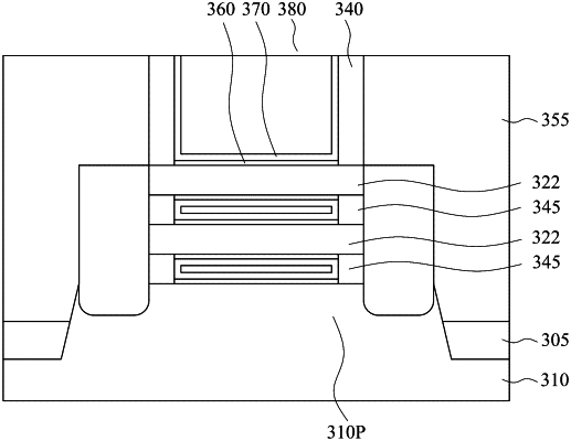
forming inner spacers vertically between two adjacent semiconductor layers;
forming source/drain structures on opposite sides of the dummy gate structure after forming the inner spacers;
removing the dummy gate structure after forming the source/drain structures;
forming an interfacial layer in contact with each of the semiconductor layer;
forming a quasi-antiferroelectric (QAFE) layer over the interfacial layer, wherein a crystalline structure of the QAFE layer is a mixture of a tetragonal phase and an orthorhombic phase, and a ratio of the tetragonal phase to the orthorhombic phase in the QAFE layer is in a range from about 1:10 to about 10:1, wherein the QAFE layer has a thickness in a range from about 8 nm to about 12 nm, wherein forming the QAFE layer comprises performing an atomic layer deposition (ALD) cycle, and the ALD cycle comprises:
performing a first sub-cycle for X time(s), wherein the first sub-cycle comprises providing a Zr-containing precursor;
performing a second sub-cycle for Y time(s), wherein the second sub-cycle comprises providing a Hf-containing precursor; and
performing a third sub-cycle for Z time(s), wherein the third sub-cycle comprises providing a Zr-containing precursor, and wherein X+Z is at least three times Y; and
forming a gate electrode over the QAFE layer so as to form a semiconductor device, wherein the semiconductor device is operable in a subthreshold swing (SS) lower than about 60 (mV/dec) and without hysteresis, wherein the QAFE layer is in direct contact with the interfacial layer, the inner spacers, the gate spacers, and the gate electrode.
|