| CPC H01L 29/7827 (2013.01) [H01L 27/1203 (2013.01); H01L 27/13 (2013.01); H01L 29/24 (2013.01); H01L 29/42356 (2013.01)] | 19 Claims |

|
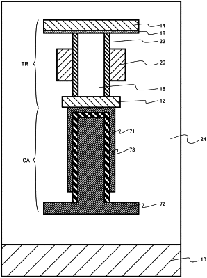
1. A semiconductor memory device comprising:
a first electrode;
a second electrode,
an oxide semiconductor layer provided between the first electrode and the second electrode, the oxide semiconductor layer being in contact with the first electrode, the oxide semiconductor layer containing zinc (Zn) and at least one first element selected from the group consisting of indium (In), gallium (Ga), silicon (Si), aluminum (Al), and tin (Sn), and a chemical composition of the oxide semiconductor layer being different from a chemical composition of the first electrode and the second electrode;
a conductive layer provided between the oxide semiconductor layer and the second electrode, the conductive layer being in contact with the second electrode, the conductive layer containing oxygen (O) and at least one second element selected from the group consisting of indium (In), gallium (Ga), silicon (Si), aluminum (Al), tin (Sn), zinc (Zn), and titanium (Ti), and a chemical composition of the conductive layer being different from a chemical composition of the first electrode, the second electrode, and the oxide semiconductor layer;
a gate electrode;
a gate insulating layer provided between the oxide semiconductor layer and the gate electrode; and
a capacitor electronically connected to the first 30 electrode.
|