| CPC H01L 29/7827 (2013.01) [H01L 29/1033 (2013.01); H01L 29/42364 (2013.01); H01L 29/66666 (2013.01)] | 20 Claims |
|
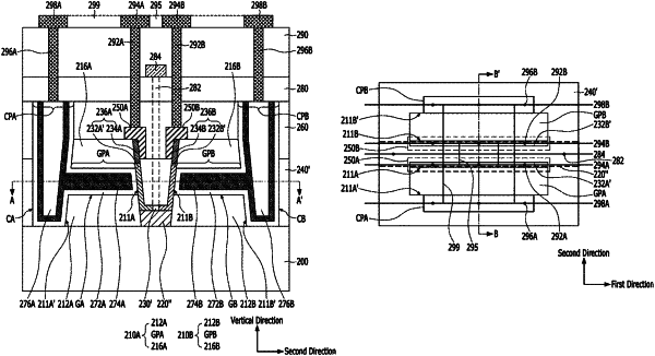
1. A semiconductor device, comprising:
a first stacked structure including a first lower dielectric layer, a first horizontal gate structure, and a first upper dielectric layer that are stacked in a vertical direction;
a second stacked structure including a second lower dielectric layer, a second horizontal gate structure, and a second upper dielectric layer that are stacked in the vertical direction, and having a first side which faces a first side of the first stacked structure;
a first channel layer formed on an upper portion of the first side of the first stacked structure;
a second channel layer formed on an upper portion of the first side of the second stacked structure;
a lower electrode layer commonly coupled to lower ends of the first and second channel layers between the first stacked structure and the second stacked structure, the lower electrode layer having a first sidewall contacting a lower portion of the first side of the first stacked structure and a second sidewall contacting a lower portion of the first side of the second stacked structure;
a first upper electrode layer coupled to an upper end of the first channel layer; and
a second upper electrode layer coupled to an upper end of the second channel layer.
|