US 11,942,543 B2
Semiconductor device structure with high voltage device
Hung-Chou Lin, Douliu (TW); Yi-Cheng Chiu, New Taipei (TW); Karthick Murukesan, Hsinchu (TW); Yi-Min Chen, Hsinchu (TW); Shiuan-Jeng Lin, Hsinchu (TW); Wen-Chih Chiang, Hsinchu (TW); Chen-Chien Chang, Zhubei (TW); Chih-Yuan Chan, Kaohsiung (TW); Kuo-Ming Wu, Hsinchu (TW); and Chun-Lin Tsai, Hsinchu (TW)
Assigned to Taiwan Semiconductor Manufacturing Company, Ltd., Hsinchu (TW)
Filed by Taiwan Semiconductor Manufacturing Company, Ltd., Hsinchu (TW)
Filed on Jun. 29, 2022, as Appl. No. 17/852,802.
Application 17/142,618 is a division of application No. 16/173,721, filed on Oct. 29, 2018, granted, now 10,892,360, issued on Jan. 12, 2021.
Application 17/852,802 is a continuation of application No. 17/142,618, filed on Jan. 6, 2021, granted, now 11,424,359.
Claims priority of provisional application 62/590,808, filed on Nov. 27, 2017.
Prior Publication US 2022/0336659 A1, Oct. 20, 2022
Int. Cl. H01L 29/78 (2006.01); H01L 29/06 (2006.01); H01L 29/08 (2006.01); H01L 29/40 (2006.01); H01L 29/423 (2006.01)
CPC H01L 29/7816 (2013.01) [H01L 29/0649 (2013.01); H01L 29/0692 (2013.01); H01L 29/0865 (2013.01); H01L 29/0869 (2013.01); H01L 29/0882 (2013.01); H01L 29/0886 (2013.01); H01L 29/402 (2013.01); H01L 29/404 (2013.01); H01L 29/42356 (2013.01); H01L 29/4238 (2013.01); H01L 29/42368 (2013.01)] 20 Claims
OG exemplary drawing
 
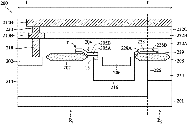
1. A semiconductor device structure, comprising:
a transistor including:
a source region in a first well region within a second well region; and
a drain region in the second well region;
a doped region having a conductivity type opposite to that of the second well region and adjacent to the second well region;
a conductor electrically connected to the transistor and extending across an interface between the doped region and the second well region; and
a shielding element ring between the conductor and the doped region, wherein the shielding element ring surrounds the transistor and extends over and across the interface.