|
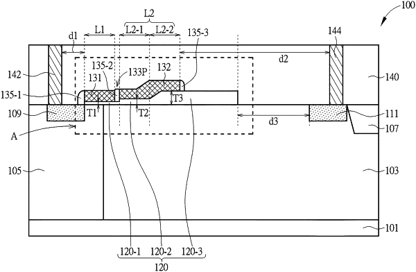
1. A semiconductor device, comprising: a substrate; a gate dielectric layer disposed on the substrate, wherein the gate dielectric layer includes a first portion having a first thickness, a second portion having a second thickness, and a third portion having a third thickness, and the first thickness, the second thickness and the third thickness are different from each other, and the first thickness is smaller than the second thickness and the third thickness; a gate electrode disposed on the first portion of the gate dielectric layer; a field plate disposed on and being in contact with top surfaces of both the second portion and the third portion of the gate dielectric layer, wherein the field plate is separated from and electrically coupled to the gate electrode; a source electrode disposed on one side of the gate electrode; and a drain electrode disposed on one side of the field plate.
|