| CPC H01L 29/7816 (2013.01) [H01L 29/0873 (2013.01); H01L 29/6656 (2013.01); H01L 29/66689 (2013.01)] | 20 Claims |
|
1. A semiconductor device, comprising:
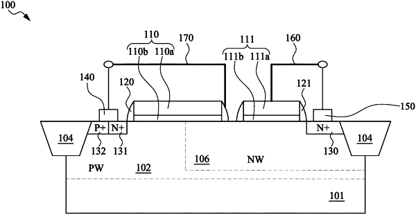
a substrate;
a source region and a drain region formed in the substrate;
a first gate structure formed on the substrate and adjacent to the source region, wherein the first gate structure has a first gate electrode and a first gate dielectric layer between the substrate and the first gate electrode;
a second gate structure formed on the substrate and adjacent to the drain region wherein the second gate structure has a second gate electrode and a second gate dielectric layer between the substrate and the second gate electrode, wherein the second gate structure is electrically coupled to the drain region via an interconnect, and wherein the first gate dielectric layer and the second dielectric layer are spaced from each other, and
a field plate formed over the first gate structure in a direction perpendicular to the substrate.
|