| CPC H01L 29/7816 (2013.01) [H01L 21/823493 (2013.01); H01L 21/823814 (2013.01); H01L 21/823857 (2013.01); H01L 21/823864 (2013.01); H01L 21/823878 (2013.01); H01L 21/823892 (2013.01); H01L 27/088 (2013.01); H01L 27/0922 (2013.01); H01L 27/0928 (2013.01); H01L 29/0623 (2013.01); H01L 29/1095 (2013.01); H01L 29/66681 (2013.01)] | 12 Claims |
|
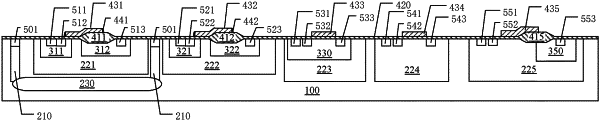
1. A semiconductor device having a laterally diffused metal oxide semiconductor (LDMOS) transistor, the semiconductor device comprising:
a high-voltage side device and a low-voltage side device;
a substrate having a first doping type and being shared by both the high-voltage side device located at a first side of the substrate, and the low-voltage side device located at a second side of the substrate;
a first deep well region having the first doping type in the first side of the substrate;
a drift region located in the first deep well region and having a second doping type;
a gate structure located on a surface of the first deep well region, wherein the gate structure comprises a drain oxide layer located on a surface of the drift region, and a gate oxide layer located on the surface of the substrate and in contact with the drain oxide layer, wherein the gate oxide layer is shared by both the high-voltage side device and the low-voltage side device; and
a drain region located in the drift region and having the second doping type, wherein the second doping type is opposite to the first doping type,
wherein a doping concentration distribution of the first deep well region has a doping concentration peak that is located below the drift region, in order to optimize the breakdown voltage and the on-resistance of the LDMOS transistor.
|