| CPC H01L 29/7813 (2013.01) [H01L 21/763 (2013.01); H01L 29/0638 (2013.01); H01L 29/407 (2013.01); H01L 29/7838 (2013.01); H01L 29/861 (2013.01)] | 15 Claims |
|
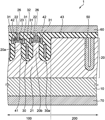
1. A semiconductor device, comprising:
an upper electrode;
a lower electrode;
a silicon substrate positioned between the upper electrode and the lower electrode, the silicon substrate being of a first conductivity type and contacting the lower electrode;
a silicon layer positioned between the silicon substrate and the upper electrode, the silicon layer including
a cell region,
a side surface, and
a termination region positioned between the cell region and the side surface;
a gate electrode located in the cell region of the silicon layer;
a gate insulating film located between the gate electrode and the silicon layer; and
a polycrystalline silicon part buried in the termination region of the silicon layer,
the polycrystalline silicon part contacting the silicon layer, having a higher crystal grain density than the silicon layer, and including a heavy metal,
the silicon layer including
a drift layer located in the cell region and the termination region, the drift layer being of the first conductivity type and having a lower first-conductivity-type impurity concentration than the silicon substrate, the drift layer including a same element of heavy metal as the heavy metal included in the polycrystalline silicon part,
a base layer located on the drift layer of the cell region, the base layer being of a second conductivity type and contacting the upper electrode, and
a source layer located on the base layer, the source layer being of the first conductivity type, contacting the upper electrode, and having a higher first-conductivity-type impurity concentration than the drift layer,
the termination region not including the base layer contacting the upper electrode, the source layer contacting the upper electrode, and the gate electrode.
|