| CPC H01L 29/7813 (2013.01) [H01L 29/1608 (2013.01)] | 13 Claims |

|
1. A silicon carbide semiconductor device comprising:
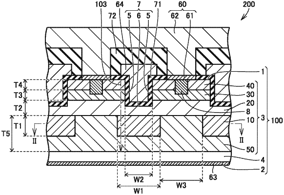
a silicon carbide substrate including a first main surface and a second main surface opposite to the first main surface, wherein
the silicon carbide substrate includes
a first impurity region containing a p-type impurity,
a second impurity region provided on the first impurity region, the second impurity region containing an n-type impurity,
a third impurity region provided on the second impurity region, the third impurity region containing a p-type impurity,
a fourth impurity region provided on the third impurity region at a distance from the second impurity region, the fourth impurity region containing an n-type impurity, and
a fifth impurity region in contact with each of the first impurity region and the second impurity region, the fifth impurity region containing an n-type impurity,
in the first main surface, a gate trench is provided, the gate trench including a side surface in contact with each of the second impurity region, the third impurity region, and the fourth impurity region and a bottom surface continuous to the side surface and being in contact with the second impurity region,
in a direction from the first main surface toward the second main surface through each of the first impurity region and the third impurity region, a concentration profile of the p-type impurity has a first relative maximum value and a third relative maximum value located closer to the first main surface than a position where the first relative maximum value is exhibited,
in the direction from the first main surface toward the second main surface through each of the second impurity region and the fourth impurity region, a concentration profile of the n-type impurity has a second relative maximum value and a fourth relative maximum value located closer to the first main surface than a position where the second relative maximum value is exhibited, and
the fourth relative maximum value is larger than the third relative maximum value, the third relative maximum value is larger than the second relative maximum value, and the second relative maximum value is larger than the first relative maximum value.
|