| CPC H01L 29/7802 (2013.01) [H01L 29/1095 (2013.01); H01L 29/2003 (2013.01); H01L 29/66522 (2013.01); H01L 29/66712 (2013.01)] | 20 Claims |
|
1. A method of fabricating a vertical FET device fabricated in GaN, the method comprising:
providing a GaN substrate comprising a surface region and a backside region;
forming an n-type GaN epitaxial layer overlying the surface region;
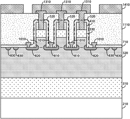
forming a plurality of finger regions, each of the finger regions having a portion of the n− type GaN epitaxial layer, an n+ type portion; and a capping layer; and configured with a plurality of recessed regions, each of the recessed regions between each pair of finger regions;
forming an n− type GaN channel comprising a doping level and a thickness selected to provide a large gate-drain breakdown voltage in a range from 100 volts to 20 kilo-volts;
forming an n+ type source configured from the n+ type portion of the finger region;
performing a selective area implant region comprising an activated impurity, selected from at least one of Be, Mg, Zn, Ca, and Cd, configured from a bottom portion of the recessed regions, and configured to be substantially free from ion implant damage using an annealing process;
forming a p-type gate region configured from the selective area implant region;
forming a depth characterizing each of the recessed regions configured to provide physical separation between the n+ type source region and the p-type gate region such that a low reverse leakage gate-source p-n junction is achieved;
forming an extended drain region configured from a portion of n− type GaN region underlying the recessed regions;
forming an n+ GaN region formed by epitaxial growth directly overlying the backside region of the GaN substrate; and
forming a backside drain contact region configured from the n+ type GaN region overlying the backside region.
|