| CPC H01L 29/7606 (2013.01) [H01L 21/8256 (2013.01); H01L 27/0922 (2013.01); H01L 29/66969 (2013.01); H01L 29/78642 (2013.01)] | 20 Claims |
|
1. A semiconductor device, comprising:
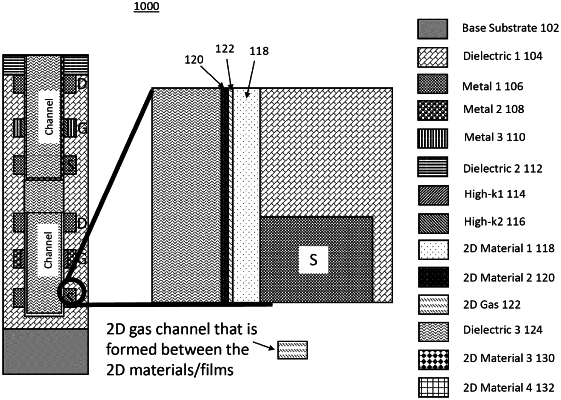
a channel structure surrounding a dielectric core, the channel structure comprising a first two-dimensional (2D) material and a second 2D material;
a source metal surrounding a first portion of the channel structure;
a drain metal surrounding a second portion of the channel structure; and
a gate metal surrounding a third portion of the channel structure.
|