| CPC H01L 29/7396 (2013.01) [H01L 29/0607 (2013.01); H01L 29/0696 (2013.01)] | 20 Claims |
|
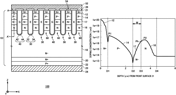
1. A semiconductor device, comprising:
a drift region that is of a first conductivity type and is provided in a semiconductor substrate;
a base region that is of a second conductivity type and is provided above the drift region;
an accumulation region that is of the first conductivity type, is provided between the base region and the drift region, and has a higher doping concentration than the drift region; and
an electric field relaxation region that is provided between the base region and the accumulation region, and has a doping concentration that is lower than a peak of the doping concentration of the accumulation region,
wherein
a boundary between the electric field relaxation region and the accumulation region is a location for a half-value for the peak of the doping concentration of the accumulation region, and
an integrated concentration of the electric field relaxation region is greater than or equal to 5E14 cm−2 and less than or equal to 5E15 cm−2.
|