| CPC H01L 29/66795 (2013.01) [H01L 21/823431 (2013.01); H01L 29/0665 (2013.01); H01L 29/785 (2013.01)] | 20 Claims |
|
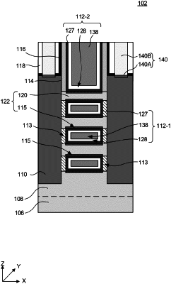
1. A method, comprising:
forming a superlattice structure comprising a plurality of first nanostructured layers and a plurality of second nanostructured layers on a substrate;
removing the plurality of second nanostructured layers to form a plurality of gate openings;
forming a germanium epitaxial layer on the plurality of first nanostructured layers at a first temperature;
performing a temperature ramping process for a first period of time to increase the first temperature to a second temperature; and
annealing the germanium epitaxial layer at the second temperature for a second period of time to form a cladding layer surrounding the plurality of first nanostructured layers.
|