| CPC H01L 29/66795 (2013.01) [H01L 21/28088 (2013.01); H01L 29/4966 (2013.01); H01L 29/66545 (2013.01); H01L 29/7851 (2013.01)] | 20 Claims |
|
1. A method of fabricating a semiconductor device, comprising:
depositing a coating layer on a first region and a second region under a loading condition such that a height of the coating layer in the first region is greater than a height of the coating layer in the second region; and
applying processing gas to the coating layer to remove an upper portion of the coating layer such that a height of the coating layer in the first region is substantially a same as a height of the coating layer in the second region,
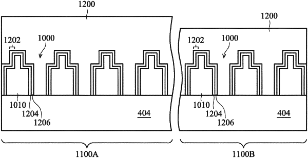
wherein the first region has first structures and first trenches adjacent the first structures, the first trenches having a first upper portion and a first lower portion, the first upper portion being wider than the first lower portion, wherein the second region has second structures and second trenches adjacent the second structures, the second trenches having a second upper portion and a second lower portion, the second upper portion being wider than the second lower portion.
|