| CPC H01L 29/66333 (2013.01) [H01L 23/4824 (2013.01); H01L 23/49562 (2013.01); H01L 24/06 (2013.01); H01L 24/49 (2013.01); H01L 25/16 (2013.01); H01L 27/0823 (2013.01); H01L 29/04 (2013.01); H01L 29/0619 (2013.01); H01L 29/0696 (2013.01); H01L 29/16 (2013.01); H01L 29/417 (2013.01); H01L 29/41708 (2013.01); H01L 29/42376 (2013.01); H01L 29/739 (2013.01); H01L 29/7397 (2013.01); H01L 29/861 (2013.01); H01L 23/4006 (2013.01); H01L 24/05 (2013.01); H01L 24/29 (2013.01); H01L 24/32 (2013.01); H01L 24/45 (2013.01); H01L 24/48 (2013.01); H01L 27/082 (2013.01); H01L 27/0825 (2013.01); H01L 29/407 (2013.01); H01L 2224/05552 (2013.01); H01L 2224/05554 (2013.01); H01L 2224/0603 (2013.01); H01L 2224/291 (2013.01); H01L 2224/32245 (2013.01); H01L 2224/45124 (2013.01); H01L 2224/48091 (2013.01); H01L 2224/48101 (2013.01); H01L 2224/48137 (2013.01); H01L 2224/48247 (2013.01); H01L 2224/48472 (2013.01); H01L 2224/4903 (2013.01); H01L 2224/49111 (2013.01); H01L 2224/49113 (2013.01); H01L 2224/49175 (2013.01); H01L 2224/73265 (2013.01); H01L 2924/1203 (2013.01); H01L 2924/13055 (2013.01); H01L 2924/13091 (2013.01); H01L 2924/181 (2013.01); H01L 2924/1815 (2013.01)] | 18 Claims |
|
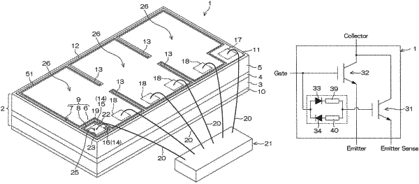
1. A semiconductor device comprising:
a semiconductor layer including a main insulated gate bipolar transistor (IGBT) cell and a sense IGBT cell connected in parallel to each other;
a first channel formed by using a gate wiring portion of the sense IGBT cell;
a first resistance portion having a first resistance value incorporated in the first channel;
a second channel formed by using the gate wiring portion of the sense IGBT cell, the second channel being a different channel from the first channel, and the second channel joining with the first channel at a gate wiring portion of the main IGBT cell;
a first diode incorporated in the first channel such that the first diode is arranged at the opposite side to the sense IGBT cell with respect to the first resistance portion;
a second resistance portion having a second resistance value higher than the first resistance value incorporated in the second channel; and
a second diode incorporated in the second channel such that the second diode is arranged at the opposite side to the sense IGBT cell with respect to the second resistance portion, the second diode provided in a manner oriented reversely to the first diode, wherein
the gate wiring portion of the sense IGBT cell includes a gate electrode formed in a predetermined wiring pattern which partitions the sense IGBT cell into cell units, and
the first resistance portion is arranged at a peripheral portion of the gate electrode.
|