| CPC H01L 29/456 (2013.01) [H01L 21/28097 (2013.01); H01L 23/535 (2013.01); H01L 29/401 (2013.01); H01L 29/42392 (2013.01); H01L 29/78696 (2013.01)] | 20 Claims |
|
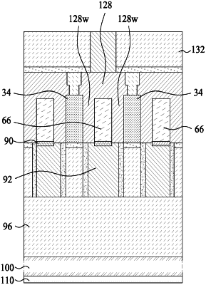
1. A semiconductor device, comprising:
a source/drain feature having a top surface, a bottom surface, and a side surface connecting the top surface and the bottom surface;
a first conductive feature disposed above the top surface of the source/drain feature and in electrical connection with the source/drain feature;
a first silicide layer formed on the top surface of the source/drain feature and in contact with the source/drain features and the first conductive feature; and
a second conductive feature having a body portion and a first sidewall portion extending from the body portion, wherein the second conductive feature is in electrical connection with the source/drain feature, the body portion is below the bottom surface of the source/drain feature, and the first sidewall portion is in contact with the first conductive feature.
|