| CPC H01L 29/42392 (2013.01) [H01L 29/0673 (2013.01); H01L 29/66545 (2013.01); H01L 29/66553 (2013.01); H01L 29/66742 (2013.01); H01L 29/7831 (2013.01); H01L 29/78696 (2013.01); H01L 21/3065 (2013.01)] | 20 Claims |
|
1. A semiconductor device, comprising:
a plurality of semiconductor layers vertically separated from one another, wherein each of the plurality of semiconductor layers extends along a first lateral direction; and
a gate structure that extends along a second lateral direction and comprises at least a lower portion that wraps around each of the plurality of semiconductor layers;
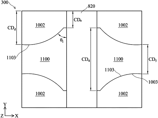
wherein the lower portion of the gate structure includes:
a plurality of first gate sections, each of the first gate sections having a first curvature-based profile when viewed from its cross-section expanding over the first and second lateral directions; and
a plurality of second gate sections, each of the second gate sections having a second, different curvature-based profile when viewed from its cross-section expanding over the first and second lateral directions.
|