| CPC H01L 29/41791 (2013.01) [H01L 21/28568 (2013.01); H01L 29/66795 (2013.01); H01L 29/7851 (2013.01)] | 20 Claims |
|
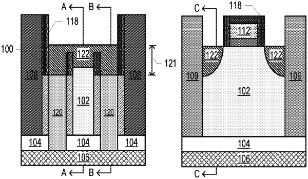
1. An integrated circuit (IC) contact structure, comprising:
an electrical element;
a metal on the electrical element;
a semiconductor material on the metal, wherein the metal conductively couples the semiconductor material and the electrical element;
a semiconductor fin between the electrical element and the semiconductor material, wherein the semiconductor material is on and in physical contact with the semiconductor fin, and wherein the semiconductor material is crystalline above the semiconductor fin, and polycrystalline above the metal; and
an insulating material between the semiconductor fin and the metal.
|