| CPC H01L 29/41733 (2013.01) [H01L 21/823814 (2013.01); H01L 27/092 (2013.01); H01L 29/0673 (2013.01); H01L 29/0847 (2013.01); H01L 29/42392 (2013.01); H01L 29/66439 (2013.01); H01L 29/6653 (2013.01); H01L 29/66545 (2013.01); H01L 29/66553 (2013.01); H01L 29/66742 (2013.01); H01L 29/775 (2013.01); H01L 29/7834 (2013.01); H01L 29/78696 (2013.01); H01L 21/30604 (2013.01); H01L 21/3065 (2013.01)] | 20 Claims |
|
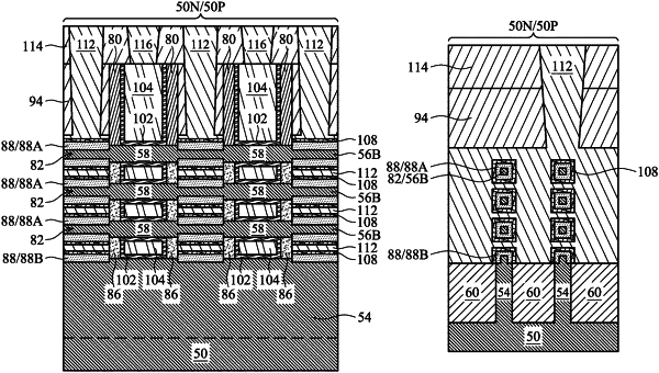
1. A device comprising:
a nanostructure comprising a lightly doped source/drain region;
an epitaxial source/drain region wrapped around a first portion of the lightly doped source/drain region, the first portion of the lightly doped source/drain region having a first thickness; and
a spacer adjacent the epitaxial source/drain region, the spacer disposed on a second portion of the lightly doped source/drain region, the second portion of the lightly doped source/drain region having a second thickness, the second thickness greater than the first thickness.
|