| CPC H01L 29/4011 (2019.08) [H01L 21/0337 (2013.01); H01L 21/3081 (2013.01); H10B 12/482 (2023.02)] | 16 Claims |
|
1. A method for manufacturing a semiconductor structure, comprising:
providing a substrate in which a plurality of active areas are arranged at intervals;
sequentially forming a first laminated structure and a first photoresist layer on the substrate;
performing Negative Type Develop (NTD) on the first photoresist layer by taking a first mask plate as a mask, to form a first pattern;
etching the first laminated structure along the first pattern, to form a second pattern in the first laminated structure; and
etching the substrate up to a preset depth by taking the first laminated structure having the second pattern as a mask, to form a recess and form a plurality of protuberances arranged at intervals on a remaining portion of the substrate, wherein the recess surrounds the protuberances, and the active areas are exposed between the protuberances,
wherein the sequentially forming the first laminated structure and the first photoresist layer on the substrate comprises:
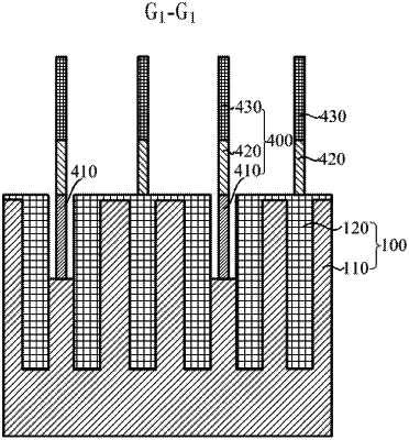
sequentially forming an insulating layer, a first conductive layer, a hard mask layer, a first mask layer and a first antireflective layer on the substrate; and
forming the first photoresist layer on the first antireflective layer,
wherein the method further comprises: after the etching the substrate up to the preset depth by taking the first laminated structure having the second pattern as the mask, to form the recess,
removing the first antireflective layer, the first mask layer and the hard mask layer, to expose the first conductive layer;
filling the recess with a second conductive layer, the second conductive layer covering the first conductive layer;
removing a part of the second conductive layer and all of the first conductive layer on the insulating layer, to enable a remaining portion of the second conductive layer to be flush with the insulating layer;
sequentially forming a third conductive layer and a protection layer on the insulating layer and the remaining portion of the second conductive layer; and
removing a part of the protection layer, a part of the third conductive layer and a part of the remaining portion of the second conductive layer, to form a plurality of bit lines arranged at intervals, wherein each of the bit lines extends along a first direction and passes through the active areas and the protuberances, the bit lines are arranged along a second direction, and the second direction is vertical to the first direction.
|
|
13. A semiconductor structure comprising a bit line formed by a method for manufacturing the semiconductor structure, wherein the method comprises:
providing a substrate in which a plurality of active areas are arranged at intervals;
sequentially forming a first laminated structure and a first photoresist layer on the substrate;
performing Negative Type Develop (NTD) on the first photoresist layer by taking a first mask plate as a mask, to form a first pattern;
etching the first laminated structure along the first pattern, to form a second pattern in the first laminated structure; and
etching the substrate up to a preset depth by taking the first laminated structure having the second pattern as a mask, to form a recess and form a plurality of protuberances arranged at intervals on a remaining portion of the substrate, wherein the recess surrounds the protuberances, and the active areas are exposed between the protuberances,
wherein the sequentially forming the first laminated structure and the first photoresist layer on the substrate comprises:
sequentially forming an insulating layer, a first conductive layer, a hard mask layer, a first mask layer and a first antireflective layer on the substrate; and
forming the first photoresist layer on the first antireflective layer,
wherein the method further comprises: after the etching the substrate up to the preset depth by taking the first laminated structure having the second pattern as the mask, to form the recess,
removing the first antireflective layer, the first mask layer and the hard mask layer, to expose the first conductive layer;
filling the recess with a second conductive layer, the second conductive layer covering the first conductive layer;
removing a part of the second conductive layer and all of the first conductive layer on the insulating layer, to enable a remaining portion of the second conductive layer to be flush with the insulating layer;
sequentially forming a third conductive layer and a protection layer on the insulating layer and the remaining portion of the second conductive layer; and
removing a part of the protection layer, a part of the third conductive layer and a part of the remaining portion of the second conductive layer, to form a plurality of bit lines arranged at intervals, wherein each of the bit lines extends along a first direction and passes through the active areas and the protuberances, the bit lines are arranged along a second direction, and the second direction is vertical to the first direction.
|