| CPC H01L 29/267 (2013.01) [H01L 21/02381 (2013.01); H01L 21/02433 (2013.01); H01L 21/02458 (2013.01); H01L 21/02505 (2013.01); H01L 21/02516 (2013.01); H01L 21/0254 (2013.01); H01L 29/045 (2013.01); H01L 29/155 (2013.01); H01L 29/7786 (2013.01); H01L 21/0262 (2013.01); H01L 21/02631 (2013.01)] | 18 Claims |
|
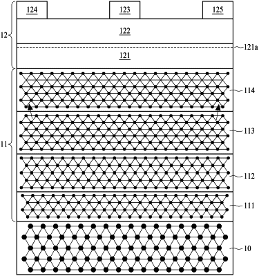
1. A semiconductor device, comprising:
a substrate;
a stack of III-nitride transition layers disposed on the substrate, the stack of III-nitride transition layers maintaining an epitaxial relationship to the substrate;
a first III-nitride layer disposed on the stack of III-nitride transition layers; and
a second III-nitride layer disposed on the first III-nitride layer, the second III-nitride layer having a band gap energy greater than that of the first III-nitride layer,
wherein the stack of III-nitride transition layers comprises a first transition layer, a second transition layer on the first transition layer, a third transition layer on the second transition layer, and a fourth transition layer sandwiched between the third transition layer and the first III-nitride layer, and
wherein the second transition layer has a minimum aluminium molar ratio among the first transition layer, the second transition layer and third transition layer; and the fourth transition layer has an aluminium molar ratio smaller than that of the third transition layer.
|