| CPC H01L 29/205 (2013.01) [H01L 29/155 (2013.01); H01L 29/2003 (2013.01); H01L 29/207 (2013.01); H01L 29/7786 (2013.01)] | 16 Claims |
|
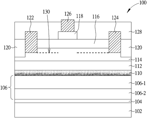
1. A semiconductor structure, comprising:
a superlattice structure, disposed on a substrate;
an electrical isolation layer, disposed on the superlattice structure;
a channel layer, disposed on the electrical isolation layer; and
a composition gradient layer, disposed between the electrical isolation layer and the superlattice structure, wherein the composition gradient layer and the superlattice structure include a same group III element, and an atomic percentage of the same group III element in the composition gradient layer is gradually decreased in a direction from the superlattice structure to the electrical isolation layer.
|