| CPC H01L 29/2003 (2013.01) [H01L 21/02381 (2013.01); H01L 21/02458 (2013.01); H01L 21/02505 (2013.01); H01L 21/0254 (2013.01); H01L 23/66 (2013.01); H01L 27/0211 (2013.01); H01L 27/0605 (2013.01); H01L 29/155 (2013.01); H01L 29/7787 (2013.01); H01L 29/872 (2013.01)] | 20 Claims |
|
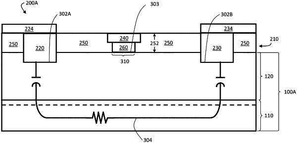
1. A semiconductor device, comprising:
a substrate;
a III-nitride material region located over the substrate;
an ohmic contact over the III-nitride material region, the ohmic contact defining an ohmic contact interfacial area with the III-nitride material region; and
a gate electrode over the III-nitride material region, the gate electrode defining a gate electrode interfacial area with the III-nitride material region, wherein
the ohmic contact interfacial area is less than 50 times the gate electrode interfacial area.
|