| CPC H01L 29/1608 (2013.01) [H01L 21/02378 (2013.01); H01L 21/02598 (2013.01)] | 14 Claims |
|
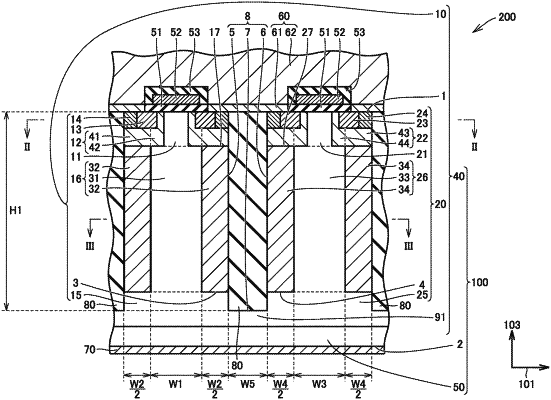
1. A silicon carbide semiconductor device comprising a silicon carbide substrate having a first main surface and a second main surface opposite to the first main surface, wherein
the silicon carbide substrate includes
a first impurity region located between the first main surface and the second main surface, the first impurity region having a first conductivity type,
a second impurity region located between the first main surface and the second main surface, the second impurity region being provided in contact with the first impurity region, the second impurity region having a second conductivity type different from the first conductivity type,
a third impurity region located between the first main surface and the second main surface, the third impurity region being provided in contact with the second impurity region so as to be separated from the first impurity region, the third impurity region having the first conductivity type,
a first superjunction portion having a first region and a second region, the first region being in contact with the first impurity region, the first region being located between the first impurity region and the second main surface, the first region having the first conductivity type, the second region being in contact with each of the second impurity region and the first region, the second region having the second conductivity type,
a fourth impurity region located between the first main surface and the second main surface, the fourth impurity region having the first conductivity type,
a fifth impurity region located between the first main surface and the second main surface, the fifth impurity region being provided in contact with the fourth impurity region, the fifth impurity region having the second conductivity type,
a sixth impurity region located between the first main surface and the second main surface, the sixth impurity region being provided in contact with the fifth impurity region so as to be separated from the fourth impurity region, the sixth impurity region having the first conductivity type, and
a second superjunction portion having a third region and a fourth region, the third region being in contact with the fourth impurity region, the third region being located between the fourth impurity region and the second main surface, the third region having the first conductivity type, the fourth region being in contact with each of the fifth impurity region and the third region, the fourth region having the second conductivity type,
the second region has a first end surface in contact with the second impurity region, and a second end surface opposite to the first end surface,
the fourth region has a third end surface in contact with the fifth impurity region, and a fourth end surface opposite to the third end surface,
the first region, the second region, the fourth region, and the third region are provided side by side in a first direction parallel to the second main surface, and
the second region is located between the first region and the fourth region, and the fourth region is located between the second region and the third region, and
the first main surface is provided with a first trench that separates the second region and the fourth region from each other,
the silicon carbide semiconductor device further comprising a first insulator provided inside the first trench, wherein
a bottom surface of the first trench is located between the second end surface and the second main surface and is located between the fourth end surface and the second main surface in a direction perpendicular to the second main surface.
|