US 11,942,516 B2
Quantum dot devices with overlapping gates
Nicole K. Thomas, Portland, OR (US); Ravi Pillarisetty, Portland, OR (US); Kanwaljit Singh, Rotterdam (NL); Hubert C. George, Portland, OR (US); David J. Michalak, Portland, OR (US); Lester Lampert, Portland, OR (US); Zachary R. Yoscovits, Beaverton, OR (US); Roman Caudillo, Portland, OR (US); Jeanette M. Roberts, North Plains, OR (US); and James S. Clarke, Portland, OR (US)
Assigned to Intel Corporation, Santa Clara, CA (US)
Filed by Intel Corporation, Santa Clara, CA (US)
Filed on Mar. 25, 2022, as Appl. No. 17/704,906.
Application 17/704,906 is a continuation of application No. 16/018,751, filed on Jun. 26, 2018, granted, now 11,335,778.
Prior Publication US 2022/0216305 A1, Jul. 7, 2022
This patent is subject to a terminal disclaimer.
Int. Cl. H01L 29/12 (2006.01); B82Y 10/00 (2011.01); G06N 10/00 (2022.01); H01L 21/02 (2006.01); H01L 21/28 (2006.01); H01L 21/306 (2006.01); H01L 21/311 (2006.01); H01L 21/324 (2006.01); H01L 23/46 (2006.01); H01L 29/10 (2006.01); H01L 29/40 (2006.01); H01L 29/423 (2006.01); H01L 29/43 (2006.01); H01L 29/66 (2006.01); H01L 29/76 (2006.01); H01L 29/778 (2006.01); H01L 29/78 (2006.01); H01L 29/82 (2006.01)
CPC H01L 29/127 (2013.01) [B82Y 10/00 (2013.01); G06N 10/00 (2019.01); H01L 21/28158 (2013.01); H01L 23/46 (2013.01); H01L 29/1033 (2013.01); H01L 29/401 (2013.01); H01L 29/423 (2013.01); H01L 29/42312 (2013.01); H01L 29/42364 (2013.01); H01L 29/437 (2013.01); H01L 29/66439 (2013.01); H01L 29/66484 (2013.01); H01L 29/66545 (2013.01); H01L 29/6656 (2013.01); H01L 29/66977 (2013.01); H01L 29/7613 (2013.01); H01L 29/7831 (2013.01); H01L 29/7845 (2013.01); H01L 21/02164 (2013.01); H01L 21/02271 (2013.01); H01L 21/30604 (2013.01); H01L 21/31111 (2013.01); H01L 21/324 (2013.01); H01L 29/66431 (2013.01); H01L 29/778 (2013.01); H01L 29/7782 (2013.01); H01L 29/82 (2013.01)] 20 Claims
OG exemplary drawing
 
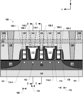
1. A quantum dot device, comprising:
a quantum well stack;
a first gate above the quantum well stack, wherein the first gate includes a first gate metal and a first gate dielectric; and
a second gate above the quantum well stack, wherein the second gate includes a second gate metal and a second gate dielectric, and the first gate is at least partially between a portion of the second gate dielectric and the quantum well stack.