| CPC H01L 29/0847 (2013.01) [H01L 21/823418 (2013.01); H01L 21/823431 (2013.01); H01L 27/0886 (2013.01); H01L 29/0653 (2013.01); H01L 29/1608 (2013.01); H01L 29/161 (2013.01); H01L 29/165 (2013.01); H01L 29/6653 (2013.01); H01L 29/66545 (2013.01); H01L 29/7848 (2013.01); H01L 29/7851 (2013.01)] | 20 Claims |
|
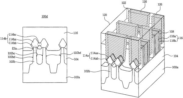
1. A semiconductor device, comprising:
a substrate;
a first active fin on the substrate, wherein the first active fin comprises a first side surface and a second side surface opposing the first side surface of the first active fin;
a second active fin on the substrate, wherein the second active fin comprises a third side surface facing the second side surface of the first active fin and a fourth side surface opposing the third side surface of the second active fin;
a third active fin on the substrate, wherein the third active fin comprises a fifth side surface facing the fourth side surface of the second active fin and a sixth side surface opposing the fifth side surface of the third active fin;
an isolation region on the substrate and comprising a first isolation layer on the first side surface of the first active fin, a second isolation layer between the second side surface of the first active fin and the third side surface of the second active fin, a third isolation layer between the fourth side surface of the second active fin and the fifth side surface of the third active fin, and a fourth isolation layer on the sixth side surface of the third active fin;
a first source/drain that extends from a top surface of the first active fin and the second active fin;
a second source/drain that extends from a top surface of the third active fin;
a first contact on and in contact with the first source/drain; and
a second contact on and in contact with the second source/drain,
wherein the first source/drain comprises:
a first portion vertically overlapping the first isolation layer;
a second portion vertically overlapping the first active fin;
a third portion vertically overlapping the second isolation layer;
a fourth portion vertically overlapping the second active fin; and
a fifth portion vertically overlapping the third isolation layer,
wherein the second source/drain comprises:
a sixth portion vertically overlapping the third isolation layer;
a seventh portion vertically overlapping the third active fin; and
an eighth portion vertically overlapping the fourth isolation layer,
wherein a first distance between the fourth side surface of the second active fin and the fifth side surface of the third active fin is greater than a second distance between the second side surface of the first active fin and the third side surface of the second active fin,
wherein the first contact comprises a first contact portion vertically overlapping the first source/drain and a second contact portion not vertically overlapping the first source/drain,
wherein a lower end of the fifth portion of the first source/drain is at a lower level than a lower end of the third portion of the first source/drain, and
wherein a lower portion of the first isolation layer vertically overlapping the second contact portion of the first contact that does not vertically overlap the first source/drain is lower than a lower surface of the second isolation layer.
|