| CPC H01L 29/0692 (2013.01) [H01L 25/072 (2013.01); H01L 25/50 (2013.01)] | 13 Claims |
|
1. A semiconductor device, comprising:
a substrate;
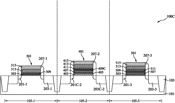
a first semiconductor stack having a first threshold voltage and comprising a first insulating stack positioned on the substrate;
a second semiconductor stack having a second threshold voltage and comprising a second insulating stack positioned on the substrate;
a third insulating stack; and
a third semiconductor stack having a third threshold voltage;
wherein the first threshold voltage is different from the second threshold voltage; a thickness of the first insulating stack is different from a thickness of the second insulating stack;
wherein the first insulating stack comprises a first bottom insulating layer positioned on the substrate and a first top conductive layer positioned above the first bottom insulating layer, wherein the first top conductive layer is made of material selected from a group consisting of aluminum, silver, titanium, titanium nitride, titanium aluminum, titanium carbide aluminum, titanium nitride aluminum, titanium silicon aluminum, tantalum nitride, tantalum carbide, tantalum silicon nitride, manganese, zirconium, or tungsten nitride,
wherein the second insulating stack comprises a second bottom insulating layer positioned on the substrate, a second middle insulating layer positioned on the second bottom insulating layer, and a second top insulating layer positioned on the second middle insulating layer, a second bottom conductive layer positioned on the second top insulating layer, a second encapsulation layer positioned on the second bottom conductive layer,
wherein the third insulating stack comprises a third bottom insulating layer positioned on the substrate and a third top insulating layer positioned on the third bottom insulating layer,
wherein the third semiconductor stack comprises a third insulating stack positioned on the substrate; and the thickness of the second insulating stack is different from the thickness of the third insulating stack,
wherein the first semiconductor stack further comprises a first bottom conductive layer positioned between the first bottom insulating layer and the first top conductive layer.
|