| CPC H01L 29/0623 (2013.01) [H01L 29/0638 (2013.01); H01L 29/402 (2013.01); H01L 29/7397 (2013.01); H02M 7/5387 (2013.01); H02P 27/06 (2013.01)] | 10 Claims |
|
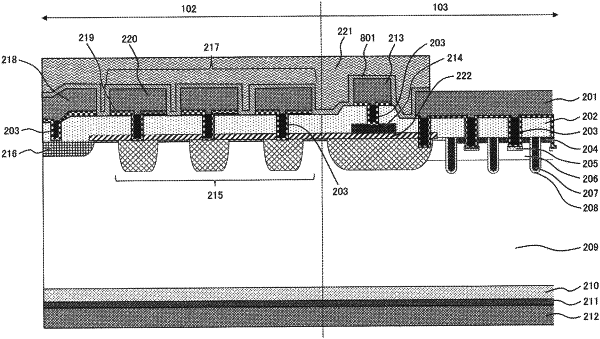
1. A semiconductor device comprising:
an active region formed on a main surface of a semiconductor substrate; and
a guard ring region formed on the main surface so as to surround the active region, wherein
the guard ring region includes:
a guard ring formed on the semiconductor substrate,
an interlayer insulating film formed on the semiconductor substrate so as to cover the guard ring,
a field plate disposed on the interlayer insulating film and electrically connected to the guard ring via a contact penetrating the interlayer insulating film, and
a protective film covering the field plate,
the field plate has a laminated structure including a first metal in contact with the guard ring and a second metal which is disposed in contact with the first metal and has a lower standard potential than the first metal, and
a ratio of a contact area of the first metal with the protective film to a contact area of the second metal with the protective film is 0.05 or less.
|