| CPC H01L 27/156 (2013.01) [H01L 33/24 (2013.01); H01L 33/385 (2013.01); H01L 33/0075 (2013.01); H01L 33/0093 (2020.05); H01L 33/12 (2013.01); H01L 33/30 (2013.01); H01L 33/42 (2013.01); H01L 33/46 (2013.01); H01L 33/62 (2013.01); H01L 2933/0016 (2013.01)] | 18 Claims |
|
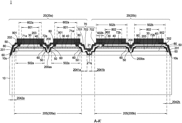
1. A light-emitting device, comprising:
a substrate;
a first light-emitting unit and a second light-emitting unit on the substrate, each of the first light-emitting unit and the second light-emitting unit comprises a first semiconductor layer, a second semiconductor layer, and an active layer between the first semiconductor layer and the second semiconductor layer, wherein the first light-emitting unit comprises a first surrounding part exposing the first semiconductor layer of the first light-emitting unit, and the second light-emitting unit comprises a second surrounding part exposing the first semiconductor layer of the second light-emitting unit;
a trench formed between the first light-emitting unit and the second light-emitting unit and exposing the substrate;
a second insulating layer comprising a first opening on the first surrounding part of the first light-emitting unit and a second opening on the second semiconductor layer of the second light-emitting unit, wherein the first opening of the second insulating layer and the second opening of the second insulating layer are aligned with each other, and the second opening of the second insulating layer comprises a first opening area larger than a second opening area of the first opening of the second insulating layer; and
a connecting electrode comprising a first connecting part formed on the first light-emitting unit and connected to the first semiconductor layer through the first opening of the second insulating layer, a second connecting part formed on the second light-emitting unit and electrically connected to the second semiconductor layer of the second light-emitting unit through the second opening of the second insulating layer, and a third connecting part formed in the trench to connect the first connecting part and the second connecting part.
|