| CPC H01L 27/156 (2013.01) [H01L 33/007 (2013.01); H01L 33/24 (2013.01); H01L 33/382 (2013.01); H01L 33/405 (2013.01); H01L 33/44 (2013.01); H01L 2933/0016 (2013.01); H01L 2933/0025 (2013.01)] | 22 Claims |
|
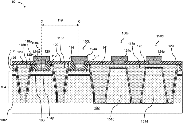
1. A light emitting diode (LED) device comprising:
a plurality of mesas defining pixels, each of the mesas comprising semiconductor layers, the semiconductor layers including an N-type layer, an active region, and a P-type layer, each of the mesas having a height less than or equal to their width;
an N-contact material in a space between each of the mesas, the N-contact material providing optical isolation between each of the mesas, and electrically contacting the N-type layer of each of the mesas along sidewalls of the N-type layers;
a dielectric material which insulates sidewalls of the P-type layer and the active region from the N-contact material; and
each of the mesas comprising a conductive p-contact layer extending across a first portion of each of the mesas and including an edge, inner spacers between the conductive p-contact layer and the dielectric material extending across a remaining portion of each of the mesas on a portion the P-type layer, and the space between each of the mesas results in a pixel pitch in a range of from 10 μm to 100 μm and a dark space gap between adjacent edges of the conductive p-contact layer of less than 20% of the pixel pitch.
|