| CPC H01L 27/14843 (2013.01) [H01L 27/14603 (2013.01); H01L 27/14607 (2013.01); H01L 27/14812 (2013.01); H04N 25/71 (2023.01); H01L 27/14831 (2013.01); H04N 25/73 (2023.01)] | 7 Claims |
|
1. A solid state imaging device comprising: a plurality of photoelectric conversion sections including photosensitive regions and distributed in a first direction, the photosensitive regions being arranged to generate a charge in response to incident light; and
a plurality of transfer sections distributed in a second direction intersecting the first direction with respect to corresponding photoelectric conversion sections of the plurality of photoelectric conversion sections and arranged to transfer the charge generated in the corresponding photoelectric conversion sections,
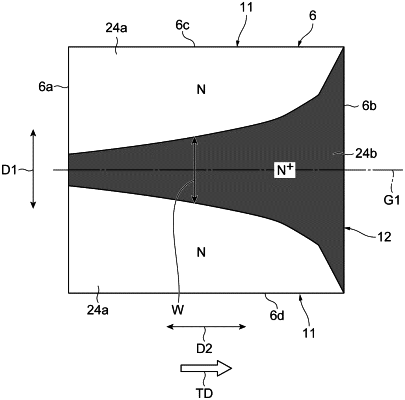
wherein the photosensitive region includes a first impurity region of a first conductivity type, a second impurity region of the first conductivity type located in a layer in which the first impurity region is located and having a higher impurity concentration than that of the first impurity region, a third impurity region of a second conductivity type, opposite the first conductivity type, located in a layer different from the layer in which the first and second impurity regions are located, and a fourth impurity region of the second conductivity type located in a layer different from the layer in which the first, second and third impurity regions are located, wherein the first and second impurity regions are between the third impurity region and the fourth impurity region, the first and second impurity regions forming a pn junction with the third impurity region, the photosensitive region including one end positioned away from the transfer section in the second direction and another end positioned closer to the transfer section in the second direction,
the second impurity region is provided from the one end of the photosensitive region or a vicinity of the one end to the other end of the photosensitive region, and has a shape that is line-symmetric with respect to a center line of the photosensitive region along the second direction in plan view, a width of the second impurity region in the first direction increases in a transfer direction from the one end to the other end, an increase rate of the width of the second impurity region in each section of a plurality of sections obtained by dividing the photosensitive region into n sections in the second direction becomes gradually higher in the transfer direction, and n is an integer of two or more,
the other end of each photosensitive region is adjacent to a corresponding transfer section of the plurality of transfer sections, and the width of the second impurity region increases up to the other end.
|