| CPC H01L 27/14636 (2013.01) [H01L 27/14634 (2013.01); H01L 27/14658 (2013.01); H01L 27/14683 (2013.01); H01L 27/1469 (2013.01); H04N 25/77 (2023.01)] | 7 Claims |
|
1. A method of constructing a flat panel image sensor, the method comprising:
mounting a plurality of image sensor chips on a substrate, wherein the substrate includes a plurality of openings, wherein each of the plurality of openings enables access to at least one image sensor unit of the plurality of image sensor units, and wherein each image sensor chip includes at least one chip contact array and wherein at least one contact of each image sensor unit is accessible through at least one opening, wherein the openings are through-holes that each correspond to a single contact of the plurality of image sensor units, optionally wherein the openings are electrically conductive through vias;
attaching a printed circuit board (“PCB”) to the substrate, wherein the PCB includes a plurality of PCB contact arrays, wherein each PCB contact array is configured to be placed in alignment and in electrical connection with a corresponding chip contact array;
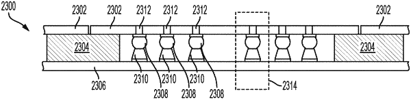
forming on each PCB contact array and each chip contact array a ball of electrically conductive adhesive paste;
aligning the substrate and the PCB so that each ball of electrically conductive adhesive paste is in contact with one electrical contact pad to form an image sensor assembly; and
curing the image sensor assembly.
|