| CPC H01L 27/14636 (2013.01) [H01L 21/76898 (2013.01); H01L 23/5226 (2013.01); H01L 25/0657 (2013.01); H01L 27/146 (2013.01); H01L 27/14623 (2013.01); H01L 27/14627 (2013.01); H01L 27/14634 (2013.01); H01L 27/14638 (2013.01); H01L 27/14645 (2013.01); H01L 27/1469 (2013.01); H04N 25/67 (2023.01); H04N 25/70 (2023.01); H04N 25/77 (2023.01); H04N 25/79 (2023.01)] | 20 Claims |
|
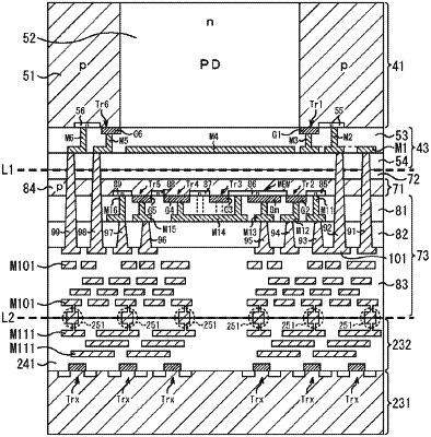
1. A solid-state imaging device, comprising:
a first semiconductor substrate and a second semiconductor substrate, a front surface side of the first semiconductor substrate forms a wiring layer formation surface of the first semiconductor substrate and joins to a back surface side of the second semiconductor substrate which is an opposite side of a wiring layer formation surface of the second semiconductor substrate,
the first semiconductor substrate including:
a photoelectric conversion portion that photoelectrically converts incident light; and
a transfer transistor that transfers an electric charge of the photoelectric conversion portion,
the second semiconductor substrate including:
a charge/voltage retention portion that retains the electric charge transferred by the transfer transistor or a voltage corresponding to the electric charge,
wherein the charge/voltage retention portion is formed within a deviation of less than 0.1 μm from a designed position;
a through electrode that penetrates the second semiconductor substrate, and transmits the electric charge transferred from the transfer transistor or the voltage to the charge/voltage retention portion,
wherein the charge/voltage retention portion is provided between the wiring layer formation surface of the first semiconductor substrate and the wiring layer formation surface of the second semiconductor substrate, and
wherein a metallic wiring line of the wiring layer formation surface of the first semiconductor substrate transmits a signal from the photoelectric conversion portion; and
a light blocking film that is in a same row as the metallic wiring line, wherein the light blocking film is positioned below the photoelectric conversion portion and above the through electrode throughout a length of the through electrode in a cross-sectional view.
|