| CPC H01L 27/14634 (2013.01) [H01L 27/14612 (2013.01); H01L 27/14623 (2013.01); H01L 27/14627 (2013.01); H01L 27/1463 (2013.01); H01L 27/14632 (2013.01); H01L 27/14636 (2013.01); H01L 27/1464 (2013.01); H01L 27/14645 (2013.01); H01L 27/14687 (2013.01); H01L 27/1469 (2013.01); H01L 31/02 (2013.01); H04N 25/76 (2023.01); H04N 25/767 (2023.01); H01L 2224/80895 (2013.01); H01L 2224/80896 (2013.01)] | 60 Claims |
|
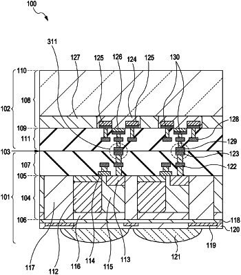
1. A photoelectric conversion apparatus comprising:
a first semiconductor layer including a photoelectric conversion element;
a second semiconductor layer including a source region and a drain region of a transistor, the transistor having a gate electrode disposed between the first semiconductor layer and the second semiconductor layer;
a first multilayer wiring structure disposed between the first semiconductor layer and the second semiconductor layer;
a second multilayer wiring structure disposed between the first multilayer wiring structure and the second semiconductor layer;
a silicide provided on at least one of the gate electrode, the drain region and the source region of the transistor;
an interlayer insulating film disposed between a first wiring layer of the second multilayer wiring structure and a second wiring layer of the second multilayer wiring structure; and
a film composed of a different material from the interlayer insulating film,
wherein a first conductor of the first multilayer wiring structure and a second conductor of the second multilayer wiring structure are bonded at a bonding surface, and
wherein at least a part of the film is located between a height of a first face of the second conductor and a height of a second face of the second conductor.
|