| CPC H01L 27/1463 (2013.01) [H01L 27/14621 (2013.01); H01L 27/14627 (2013.01); H01L 27/14645 (2013.01); H01L 27/14685 (2013.01); H01L 27/14689 (2013.01); H04N 25/704 (2023.01); H04N 25/79 (2023.01)] | 16 Claims |
|
1. An image sensor comprising:
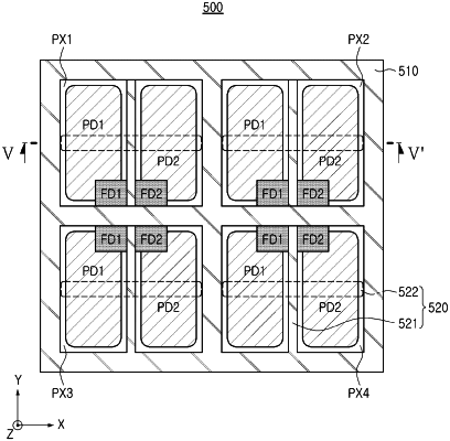
a pixel array including a substrate, a plurality of pixels arranged in directions parallel to an upper surface of the substrate, and a pixel isolation layer between the plurality of pixels, each of the plurality of pixels including at least one photodiode and a pixel circuit below the at least one photodiode; and
a logic circuit configured to acquire a pixel signal from the plurality of pixels,
wherein the pixel array comprises at least one autofocusing pixel,
wherein the at least one autofocusing pixel comprises a first photodiode, a second photodiode, a pixel internal isolation layer between the first photodiode and the second photodiode, and a microlens on the first photodiode and the second photodiode,
wherein the pixel internal isolation layer includes a first pixel internal isolation layer and a second pixel internal isolation layer,
the first pixel internal isolation layer and the second pixel internal isolation layer are separated from each other in a first direction,
the first direction is perpendicular to the upper surface of the substrate,
a material of the first pixel internal isolation layer is different than a material of the second pixel internal isolation layer,
wherein the second pixel internal isolation layer does not overlap the first photodiode and the second photodiode in a second direction and a third direction, and
wherein the first direction, the second direction, and third direction are different from each other and perpendicular to each other, and
wherein a first surface of the substrate is a lower surface of the substrate and a second surface of the substrate is opposite the first surface of the substrate,
wherein the second pixel internal isolation layer comprises an insulating material, and
wherein the second pixel internal isolation layer has a third surface and a fourth surface parallel to the first surface, the third surface is separated from the first photodiode and the second photodiode in the first direction, and the third surface is co-planar with the second surface.
|