| CPC H01L 27/14625 (2013.01) [H01L 27/1207 (2013.01); H01L 27/1225 (2013.01); H01L 27/1229 (2013.01); H01L 27/14601 (2013.01); H01L 27/14612 (2013.01); H01L 27/14616 (2013.01); H01L 27/14623 (2013.01); H01L 27/14634 (2013.01); H01L 27/14636 (2013.01); H01L 27/14643 (2013.01); H01L 27/14689 (2013.01); H01L 27/1469 (2013.01); H01L 27/14692 (2013.01); H01L 29/78 (2013.01); H01L 29/7869 (2013.01); H01L 2224/80895 (2013.01); H01L 2224/80896 (2013.01)] | 10 Claims |
|
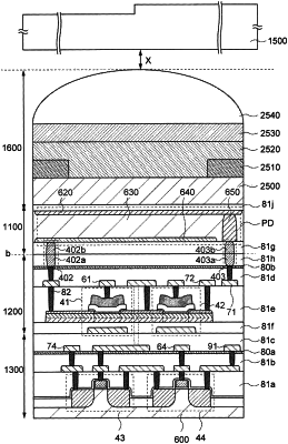
6. An imaging device comprising:
a first layer including a transistor, and a first metal layer and a second metal layer over the transistor;
a second layer including a third metal layer and a fourth metal layer, and a photoelectric conversion element over the third metal layer and the fourth metal layer; and
a third layer including a first light-blocking layer and a second light-blocking layer,
wherein the second layer is provided over the first layer, and the third layer is provided over the second layer,
wherein the first metal layer is electrically connected to one of a source and a drain of the transistor,
wherein the fourth metal layer is electrically connected to one electrode of the photoelectric conversion element,
wherein the third metal layer is in direct contact with the first metal layer at a first connection portion, and the fourth metal layer is in direct contact with the second metal layer at a second connection portion,
wherein the first light-blocking layer overlaps the first connection portion and the second light-blocking layer overlaps the second connection portion, and
wherein each of the first metal layer, the second metal layer, the third metal layer and the fourth metal layer contains copper.
|