| CPC H01L 27/14618 (2013.01) [H01L 27/14636 (2013.01); H01L 27/14683 (2013.01); H01L 31/024 (2013.01)] | 26 Claims |
|
1. A semiconductor device, comprising:
a semiconductor chip;
a circuit board configured to transmit a signal of the semiconductor chip;
a heat releasing plate, wherein
the semiconductor chip is on the heat releasing plate, and
the heat releasing plate includes:
a semiconductor chip placement region and a first opening in a first region on an outer side of the semiconductor chip placement region, wherein
the semiconductor chip placement region is in contact with the circuit board, and
the semiconductor chip is on the semiconductor chip placement region; and
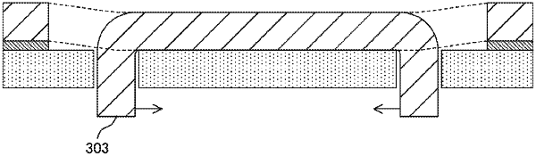
a protrusion configured to lock the semiconductor chip placement region to the circuit board so as to bring the semiconductor chip placement region into contact with the circuit board;
an adhesive member configured to bond the circuit board and the heat releasing plate, wherein
the adhesive member is in a region on an outer side of the first opening on a first surface of the heat releasing plate,
the first surface of the heat releasing plate is different from a second surface of the heat releasing plate, and
the semiconductor chip is on the second surface of the heat releasing plate; and
a conductive member configured to connect the semiconductor chip with the circuit board via the first opening.
|