| CPC H01L 27/14618 (2013.01) [H04N 23/54 (2023.01); H04N 23/55 (2023.01)] | 14 Claims |
|
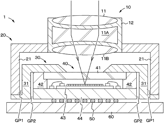
1. An imaging device, comprising:
a wiring substrate;
an image sensor package mounted on the wiring substrate;
a package frame attached to a light receiving surface side of the image sensor package; and
a lens holder arranged to:
cover the package frame, and
hold a lens unit so that the lens unit faces the light receiving surface of the image sensor package, wherein
the package frame includes a material having a larger coefficient of linear expansion than a material of the lens holder, and includes a wall portion that extends in a direction perpendicular to the wiring substrate toward the wiring substrate,
a gap is provided between the wall portion of the package frame and the image sensor package, and between an end of the wall portion of the package frame and the wiring substrate,
the lens holder includes a wall portion facing the wall portion of the package frame, and
an end of the wall portion of the lens holder is fixed to the end of the wall portion of the package frame while being separated from the wiring substrate.
|