| CPC H01L 27/14616 (2013.01) [H01L 27/14603 (2013.01); H01L 27/14614 (2013.01); H01L 27/14689 (2013.01); H04N 25/75 (2023.01); H01L 27/14645 (2013.01); H04N 25/77 (2023.01)] | 8 Claims |
|
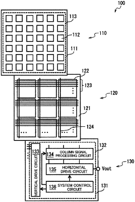
1. An imaging device, comprising:
a light receiving element; and
a read circuit configured to read an electrical signal photoelectrically converted by the light receiving element,
wherein a field effect transistor included in the read circuit includes
a semiconductor layer in which a channel is formed,
a gate electrode configured to cover the semiconductor layer, and
a gate insulating film disposed between the semiconductor layer and the gate electrode,
the semiconductor layer includes
a main surface, and
a first side surface located on one end side of the main surface in a gate width direction of the field effect transistor,
the gate electrode includes
a first portion configured to face the main surface via the gate insulating film, and
a second portion configured to face the first side surface via the gate insulating film, and
a crystal plane of the first side surface is a (100) plane or a plane equivalent to the (100) plane.
|