| CPC H01L 27/124 (2013.01) [H01L 27/1262 (2013.01); H10K 59/131 (2023.02)] | 5 Claims |
|
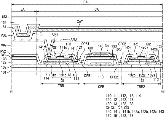
1. A method of fabricating a display device comprising a plurality of pixels and a first transistor and a second transistor in each of the pixels, the method comprising:
forming a first conductive layer, which comprises a first power wiring electrically connected to a first source/drain electrode of the first transistor, a lower light blocking pattern electrically connected to a second source/drain electrode of the first transistor and a data wiring electrically connected to a first source/drain electrode of the second transistor, on a substrate;
sequentially coating an insulating layer material, a semiconductor layer material and a gate insulating layer material on the substrate to cover the first conductive layer; and
etching the gate insulating layer material, the semiconductor layer material and the insulating layer material by using a halftone mask to pattern a gate insulating layer which comprises a gate insulating layer of the first transistor and a gate insulating layer of the second transistor, a semiconductor layer which comprises a semiconductor pattern of the first transistor and a semiconductor pattern of the second transistor, and an insulating layer which comprises a first insulating pattern having the same planar shape as the semiconductor pattern of the first transistor and a second insulating pattern having a same planar shape as the semiconductor pattern of the second transistor.
|