| CPC H01L 27/124 (2013.01) | 20 Claims |
|
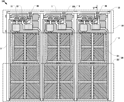
1. An array substrate, comprising a plurality of rows of pixel units, wherein
each of the pixel units is provided with a transistor area; a main transistor unit, a sub-transistor unit, and a shared transistor unit are disposed in the transistor area; and the shared transistor unit comprises a source and a drain;
each of the plurality of rows of the pixel units is provided with a shared metal wiring; and the shared metal wiring is provided above the transistor area and extends along an arrangement direction of the pixel units in a corresponding one of the plurality of rows, and is electrically connected to the source of the shared transistor unit in each of the pixel units, sequentially.
|