| CPC H01L 27/1225 (2013.01) [H01L 27/1248 (2013.01); H01L 29/045 (2013.01); H01L 29/786 (2013.01); H01L 29/78648 (2013.01); H01L 29/7869 (2013.01); H01L 27/1259 (2013.01); H01L 27/1262 (2013.01); H10K 59/1213 (2023.02); H10K 59/123 (2023.02)] | 6 Claims |
|
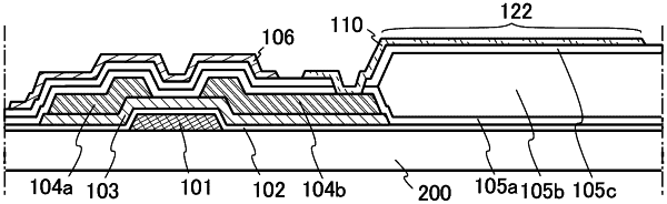
1. A display device comprising:
a first conductive layer and a second conductive layer over a substrate;
a third conductive layer configured to be a gate electrode of a transistor;
an insulating layer over a channel of the transistor; and
a pixel electrode and a fourth conductive layer over the insulating layer,
wherein the first conductive layer is made of a same conductive material as the second conductive layer and the third conductive layer,
wherein the pixel electrode is made of a same transparent conductive material as the fourth conductive layer,
wherein the channel includes an oxide semiconductor layer,
wherein the pixel electrode is electrically connected to one of a source electrode and a drain electrode of the transistor,
wherein the fourth conductive layer is electrically connected to the first conductive layer,
wherein the insulating layer includes a first region, a second region and a third region,
wherein the channel overlaps with the first region,
wherein the second conductive layer overlaps with the third region,
wherein a thickness of the second region is larger than a thickness of the first region,
wherein the thickness of the second region is larger than a thickness of the third region,
wherein the pixel electrode overlaps with the second region and the third region, and
wherein the fourth conductive layer overlaps with the first region and the second region.
|