| CPC H01L 27/1225 (2013.01) [H01L 29/7869 (2013.01); H01L 29/78696 (2013.01); H10K 59/1201 (2023.02)] | 20 Claims |
|
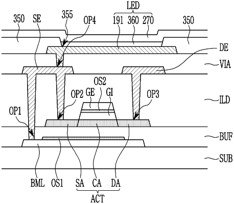
10. A display device comprising:
a light blocking layer disposed on a substrate;
a first oxygen supply layer disposed on and contacting the light blocking layer;
a semiconductor layer disposed on the first oxygen supply layer;
a gate insulating layer disposed on the semiconductor layer;
a second oxygen supply layer disposed on the gate insulating layer;
a gate electrode disposed on the second oxygen supply layer; and
a light emitting diode electrically connected with the semiconductor layer, wherein
the semiconductor layer comprises an oxide semiconductor,
the first oxygen supply layer and the second oxygen supply layer comprise a metal oxide that includes at least one of indium, zinc, gallium, and tin, and
a thickness of the first oxygen supply layer and a thickness of the second oxygen supply layer are in a range of about 30% to about 50% of a thickness of the semiconductor layer.
|