US 11,942,481 B2
Display device including polycrystalline silicon layer, method of manufacturing polycrystalline silicon layer, and method of manufacturing display device
Dong-Sung Lee, Hwaseong-si (KR); Jongoh Seo, Seoul (KR); Byung Soo So, Yongin-si (KR); Dong-min Lee, Yongin-si (KR); Yeon Hee Jeon, Hwaseong-si (KR); and Jonghoon Choi, Hwaseong-si (KR)
Assigned to SAMSUNG DISPLAY CO., LTD., Yongin-si (KR)
Filed by Samsung Display Co., LTD., Yongin-si (KR)
Filed on Oct. 26, 2021, as Appl. No. 17/510,995.
Application 17/510,995 is a division of application No. 16/821,484, filed on Mar. 17, 2020, granted, now 11,183,515.
Claims priority of application No. 10-2019-0031324 (KR), filed on Mar. 19, 2019.
Prior Publication US 2022/0045105 A1, Feb. 10, 2022
This patent is subject to a terminal disclaimer.
Int. Cl. H01L 21/00 (2006.01); H01L 21/02 (2006.01); H01L 27/12 (2006.01); H01L 29/04 (2006.01); H01L 29/786 (2006.01)
CPC H01L 27/1222 (2013.01) [H01L 21/02592 (2013.01); H01L 21/02675 (2013.01); H01L 27/1274 (2013.01); H01L 29/045 (2013.01); H01L 29/78675 (2013.01)] 12 Claims
OG exemplary drawing
 
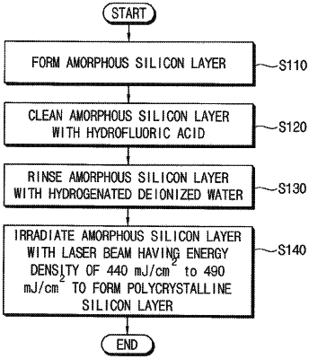
1. A method of manufacturing a polycrystalline silicon layer, comprising:
forming an amorphous silicon layer on a substrate;
cleaning the amorphous silicon layer with hydrofluoric acid;
rinsing the amorphous silicon layer with hydrogenated deionized water; and
irradiating the amorphous silicon layer with a laser beam having an energy density in a range of about 440 mJ/cm2 to about 490 mJ/cm2 to form the polycrystalline silicon layer.