| CPC H01L 27/1203 (2013.01) [H01L 21/84 (2013.01); H01L 29/1083 (2013.01); H01L 29/78648 (2013.01); H01L 23/535 (2013.01)] | 10 Claims |
|
1. A semiconductor device comprising:
a substrate;
a first buried insulation layer disposed on the substrate;
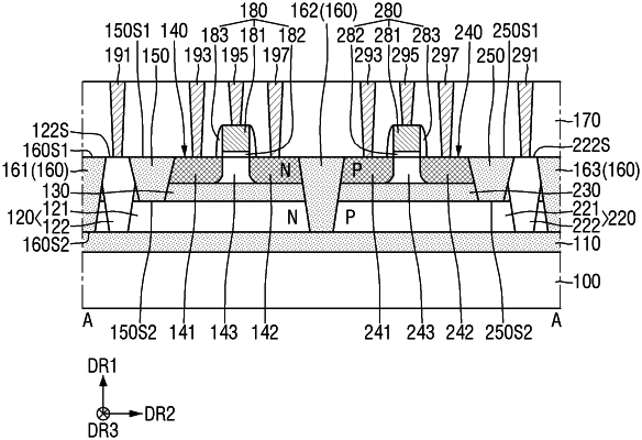
a first well which is disposed on the first buried insulation layer in a first region defined by a first element separation film, and comprises a first portion extending along an upper surface of the first buried insulation layer, and a second portion extending from the first portion in a direction from the substrate toward the first buried insulation layer;
a second buried insulation layer disposed on the first portion of the first well;
a first semiconductor film disposed on the second buried insulation layer;
a first transistor on the first semiconductor film;
a second element separation film which separates the first semiconductor film from the second portion of the first well on the first portion of the first well;
a second well which is disposed on the first buried insulation layer in a second region being adjacent to the first region and defined by the first element separation film, and comprises a third portion extending along the upper surface of the first buried insulation layer, and a fourth portion extending from the third portion in the direction;
a third buried insulation layer disposed on the third portion of the second well;
a second semiconductor film disposed on the third buried insulation layer;
a second transistor disposed on the second semiconductor film; and
a third element separation film which separates the second semiconductor film from the fourth portion of the second well on the third portion of the second well,
wherein the first well, the second buried insulation layer and the first semiconductor film are completely separated from the second well, the third buried insulation layer and the second semiconductor film, respectively, by the first element separation film, and
wherein an upper surface of the second portion of the first well is placed on the same plane as an upper surface of the first element separation film.
|