| CPC H01L 27/0886 (2013.01) [H01L 21/31111 (2013.01); H01L 21/31116 (2013.01); H01L 21/76224 (2013.01); H01L 21/823418 (2013.01); H01L 21/823431 (2013.01); H01L 21/823437 (2013.01); H01L 21/823481 (2013.01); H01L 27/0207 (2013.01); H01L 29/0847 (2013.01); H01L 29/66545 (2013.01); H01L 29/7848 (2013.01); H01L 21/0217 (2013.01); H01L 21/02271 (2013.01); H01L 21/0228 (2013.01); H01L 21/0274 (2013.01); H01L 21/0332 (2013.01); H01L 21/31053 (2013.01); H01L 21/32139 (2013.01); H01L 29/165 (2013.01); H01L 29/205 (2013.01)] | 20 Claims |

|
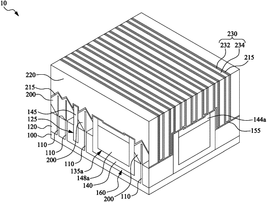
1. A method, comprising:
forming a semiconductor fin on a substrate;
conformally forming a dielectric layer over the semiconductor fin;
depositing an oxide layer over the dielectric layer;
etching back the oxide layer to lower a top surface of the oxide layer to a level below a top surface of the semiconductor fin;
conformally forming a metal oxide layer over the semiconductor fin, the dielectric layer, and the etched back oxide layer;
planarizing the metal oxide layer and the dielectric layer to expose the semiconductor fin;
forming a gate structure extending across the semiconductor fin; and
forming source/drain regions on the semiconductor fin and on opposite sides of the gate structure.
|