| CPC H01L 27/0886 (2013.01) [H01L 21/02164 (2013.01); H01L 21/02532 (2013.01); H01L 21/02595 (2013.01); H01L 21/28052 (2013.01); H01L 21/823431 (2013.01); H01L 21/823443 (2013.01); H01L 21/823456 (2013.01); H01L 21/823468 (2013.01); H01L 27/088 (2013.01); H01L 29/401 (2013.01); H01L 29/42364 (2013.01); H01L 29/42376 (2013.01); H01L 29/4933 (2013.01); H01L 29/66795 (2013.01); H01L 29/785 (2013.01)] | 20 Claims |

|
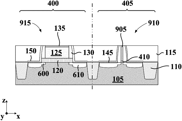
1. A structure, comprising:
a first transistor formed on a first region of a semiconductor substrate, wherein the first transistor comprises:
a first source/drain region in the semiconductor substrate;
a lightly doped region of the semiconductor substrate;
a gate dielectric disposed above the semiconductor substrate;
a polysilicon gate electrode disposed on the gate dielectric, wherein the gate dielectric is longer than the polysilicon gate electrode, and wherein an edge of the gate dielectric coincides with an edge of the lightly doped region; and
a first spacer structure abutting a sidewall of the polysilicon gate electrode; and
a second transistor having a length shorter than that of the first transistor and formed on a second region of the semiconductor substrate, wherein the second transistor comprises:
a high-k gate dielectric;
a metal gate electrode;
a second spacer structure abutting sidewalls of the metal gate electrode and the high-k gate dielectric; and
a second source/drain region substantially co-planar with the first source/drain region and in direct contact with a bottom surface of the second spacer structure.
|