| CPC H01L 27/088 (2013.01) [H01L 21/77 (2013.01); H01L 25/0657 (2013.01); H01L 29/66712 (2013.01); H01L 29/7802 (2013.01)] | 7 Claims |
|
1. A method of manufacturing a parallel structure of semiconductor devices, comprising:
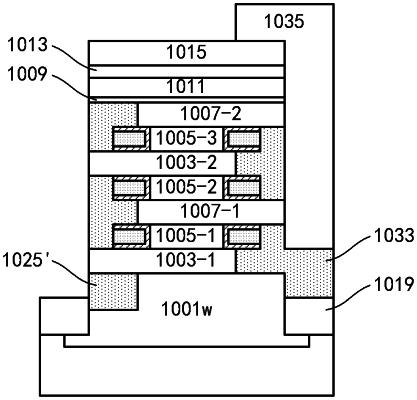
disposing a semiconductor stack on a substrate, wherein the semiconductor stack comprises a plurality of source/drain layers disposed sequentially in a vertical direction and two or more channel layers respectively disposed between respective pairs of adjacent ones of the source/drain layers;
patterning the semiconductor stack into a predetermined shape to define an active region;
forming gate stacks around at least part of outer peripheries of the respective channel layers;
forming an isolation layer on outer peripheries of the active region and the gate stack; and
forming a first electrically conductive channel, a second electrically conductive channel and a third electrically conductive channel on a sidewall of the isolation layer,
wherein, the method further comprises determining the pre-determined shape and a shape of the formed gate stacks, such that in each of the semiconductor devices, one of the source/drain layers on upper and lower sides of the corresponding channel layer passes through the isolation layer to contact the first electrically conductive channel, while the other one passes through the isolation layer to contact the second electrically conductive channel, and the corresponding gate stack passes through the isolation layer to contact the third electrically conductive channel.
|